Many projects in this section of the forum focus on exceptional, wire-like performance, often based on class-A, single-ended or zero GNFB topologies (and sometimes all of them).
As a result, they are hefty, power-hungry projects considering their smallish output power.
The BoosterPhone is the exact counterpoint of that philosophy: it offers decent performances, but not much more. For example, the THD is 0.1% and the full power bandwidth is 100kHz, which is OK but certainly not exceptional.
The BoosterPhone focusses on other aspects: convenience, practicality, usability and usefulness.
It achieves that by being a quasi-passive box, with only an input and an output and no controls.
It cannot be fully passive, unlike a transformer for example, but it is autonomous and so frugal and effective that it mostly looks like a passive device.
One of its most important feature is the absence of a power switch: the current consumption is low enough to leave it permanently On.
Its purpose is to raise the level of weak modern devices for low efficiency headphones or plugs, or to convert a line level into a low-impedance output compatible with a 32 ohm load. It was inspired by Daniel (danielwritesbac) who was looking for a simplistic solution for similar problems.
Daniel was more interested in pure line-level amplification, but this project can also work that way, by using a 100 ohm dummy load instead of the heaadphones.
My use is mostly headphone-oriented.
Basically, the BoosterPhone is a 4x gain-block (12dB), having an input impedance of ~10K, and an output impedance of a fraction of an ohm.
It is a class-B amplifier, inspired from the TracerPhone, but beefed-up to 7 transistor, and capable of operating at extremely low quiescent currents (80µA for the OP, 160µA for the whole amplifier) whilst offering a rail-to-rail capability driving a low-impedance load: with a 3.5V supply, it clips at 3.3Vpp.
As usual with my projects, it uses exclusively the most common, jelly-bean type transistors: 2SC1815 and 2SA1015 for the signal part, and S8050 for the OP, all from the cheapest Chinese sources.
The output configuration is circlo-like, and uses same sex transistors.
The nominal supply voltage can be 3.5V to 4V, making it compatible with 3 NiMh cells, or a single Li-ion cell, which I opted for. I also included a BMS suite for the Lithium, to take care of the charging and voltage monitoring.
This is the schematic of the amplifier:

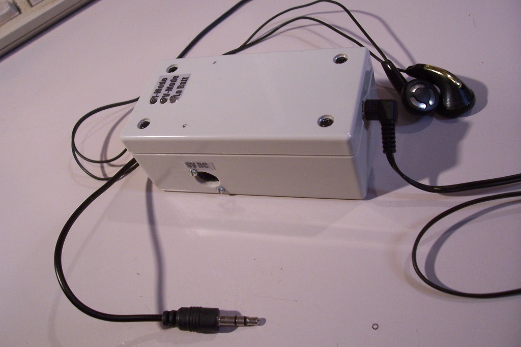
This is the finished Boosterphone:
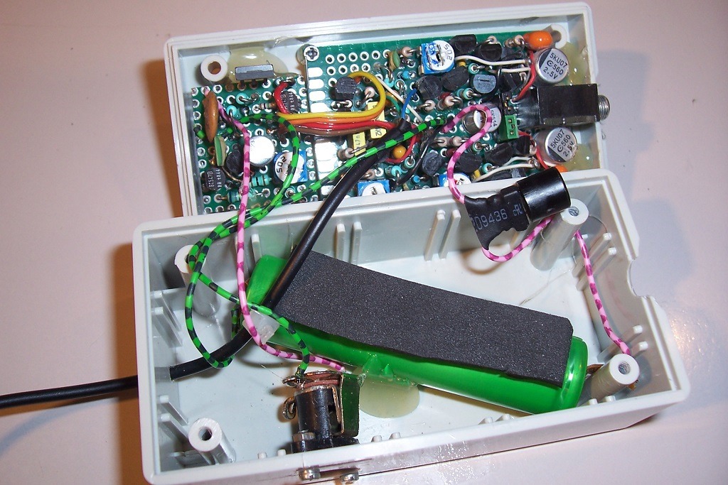
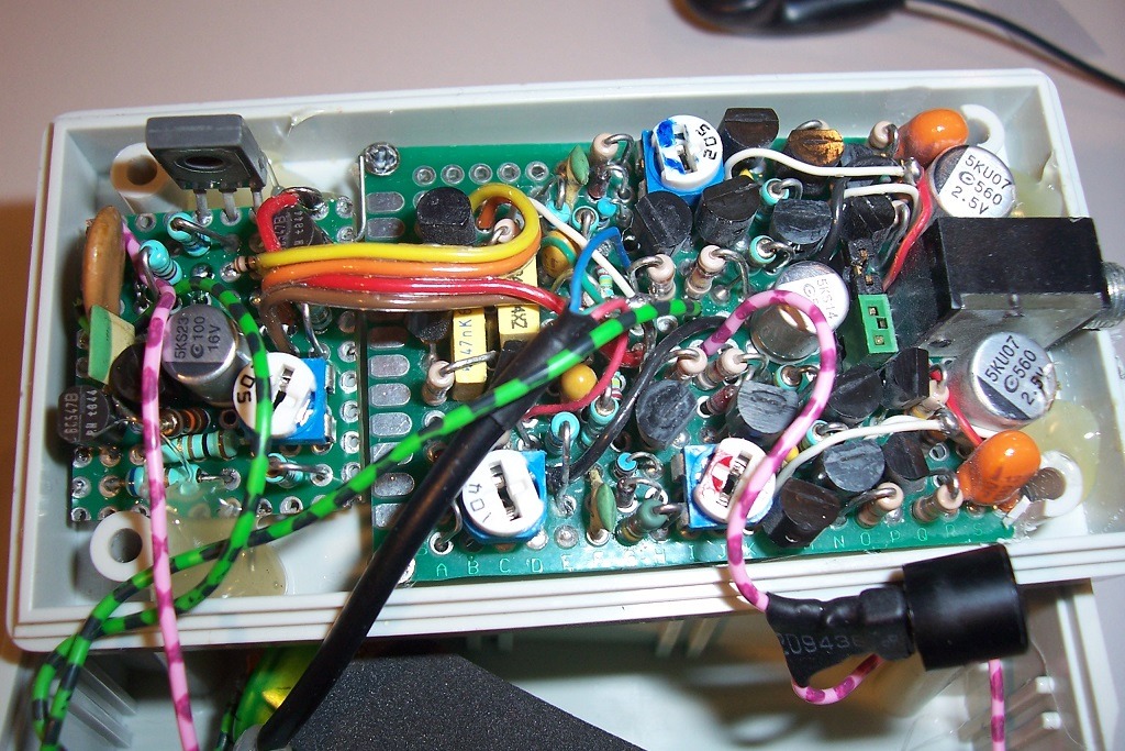
Some pics of its innards:
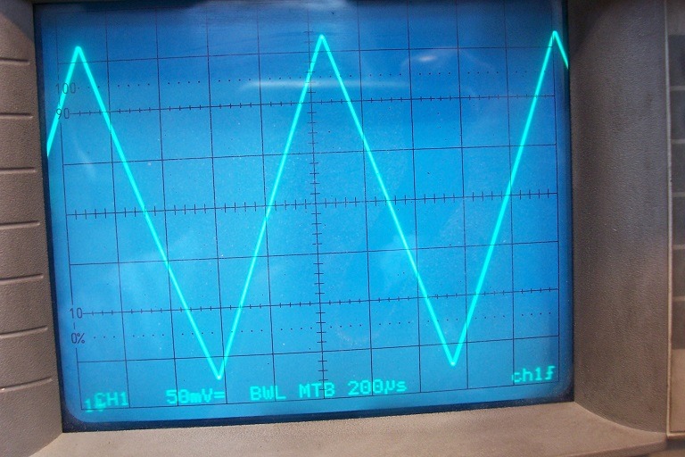
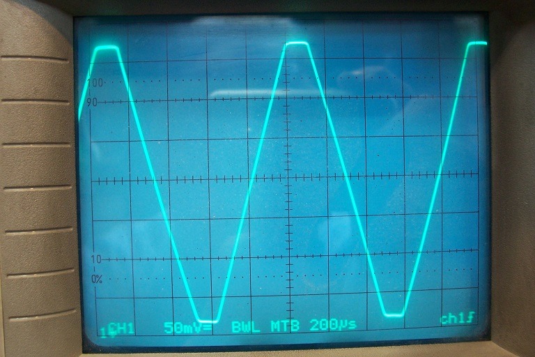
A pic of the output waveform, with a triangle wave. A hint of Xover distortion should be visible, but it is so faint as to be completely invisible on the photo: you need to look at the O-scope screen directly, with great attention to detect it (and you need to know where to look).
The clipping behaviour with a 3.8V supply (the bottom line of the graticule is 0V):
I also include a sim (not completely up to date)
As a result, they are hefty, power-hungry projects considering their smallish output power.
The BoosterPhone is the exact counterpoint of that philosophy: it offers decent performances, but not much more. For example, the THD is 0.1% and the full power bandwidth is 100kHz, which is OK but certainly not exceptional.
The BoosterPhone focusses on other aspects: convenience, practicality, usability and usefulness.
It achieves that by being a quasi-passive box, with only an input and an output and no controls.
It cannot be fully passive, unlike a transformer for example, but it is autonomous and so frugal and effective that it mostly looks like a passive device.
One of its most important feature is the absence of a power switch: the current consumption is low enough to leave it permanently On.
Its purpose is to raise the level of weak modern devices for low efficiency headphones or plugs, or to convert a line level into a low-impedance output compatible with a 32 ohm load. It was inspired by Daniel (danielwritesbac) who was looking for a simplistic solution for similar problems.
Daniel was more interested in pure line-level amplification, but this project can also work that way, by using a 100 ohm dummy load instead of the heaadphones.
My use is mostly headphone-oriented.
Basically, the BoosterPhone is a 4x gain-block (12dB), having an input impedance of ~10K, and an output impedance of a fraction of an ohm.
It is a class-B amplifier, inspired from the TracerPhone, but beefed-up to 7 transistor, and capable of operating at extremely low quiescent currents (80µA for the OP, 160µA for the whole amplifier) whilst offering a rail-to-rail capability driving a low-impedance load: with a 3.5V supply, it clips at 3.3Vpp.
As usual with my projects, it uses exclusively the most common, jelly-bean type transistors: 2SC1815 and 2SA1015 for the signal part, and S8050 for the OP, all from the cheapest Chinese sources.
The output configuration is circlo-like, and uses same sex transistors.
The nominal supply voltage can be 3.5V to 4V, making it compatible with 3 NiMh cells, or a single Li-ion cell, which I opted for. I also included a BMS suite for the Lithium, to take care of the charging and voltage monitoring.
This is the schematic of the amplifier:
This is the finished Boosterphone:
Some pics of its innards:
A pic of the output waveform, with a triangle wave. A hint of Xover distortion should be visible, but it is so faint as to be completely invisible on the photo: you need to look at the O-scope screen directly, with great attention to detect it (and you need to know where to look).
The clipping behaviour with a 3.8V supply (the bottom line of the graticule is 0V):
I also include a sim (not completely up to date)
Attachments
Member
Joined 2009
Paid Member
Interesting design. Looks like a common emitter amplifier feeding a JLH-Follower but yet it's more....
I started looking at the JLH-Follower topology but got too lazy to build!
https://www.diyaudio.com/community/threads/biguns-botch-up-amplifier.159780/
I started looking at the JLH-Follower topology but got too lazy to build!
https://www.diyaudio.com/community/threads/biguns-botch-up-amplifier.159780/
Do not be too impatient, here it is:
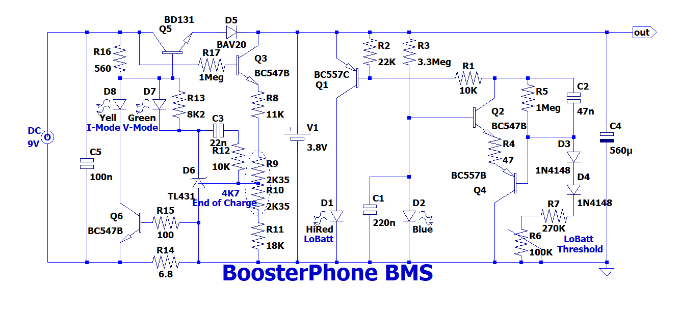
The charging section has all the features to safely charge a Li-Ion cell, since the consequences of an inadequate charging could be catastrophic.
The discharge monitoring is simplified, it does not cut off the supply, it just flashes a red LED when the threshold limit is reached. Because of the very low current drain, the battery lasts for thousands of hours, meaning you have plenty of time to react: weeks at least. Even if you don't react, you will simply hurt the capacity of the cell.
I will come back later on the details of the circuit, but first let's return to the amplifier:
It is optimized for a very low consumption, and a high efficiency, but this comes at a cost, and it has some quirks:
-It is inverting. Most people, including myself don't mind in the least, but some purists might find it objectionable
-The input and output grounds are tied to opposite polarities of the supply. For a headphone, this is of no importance, but if you use this in a complex setup where the grounds end up being connected somewhere, it will cause a short. Note that on my prototype, the output jack is recessed and the input pigtail is just too short to allow a short. It would be possible to use the negative side as GND of the output for line-level applications, but the supply needs to be perfectly clean (not too difficult with a battery supply and a good bypass though)
-The bias of the amplifier is essentially a Vbe multiplier of the input transistor. This means that the quiescent output voltage will stay constant even if the supply voltage varies, and the voltage will be the optimum Vcc/2 for only one supply voltage. It will also vary slightly with temperature
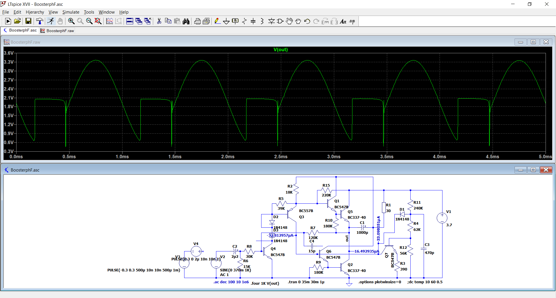
-The peculiar totem-pole configuration of the output makes it susceptible to latchup when it clips on the negative side: the phase-shifter driver/becomes saturated and the input transistor steals all the drive current from the OP, making it go tristate, which is extremely violent and requires countermeasures: I have opted for D2 and D3, but other methods are also usable.
This sim shows the phenomenon and its violence; the reality is exactly identical:
-The nominal bias current of the output is 80µA. At such a level, the dynamic resistance of the emitter junction is ~320 ohm, ten times the load! But it doesn't end there: the input transistor of the darlington contributes to the same amount when scaled, and the totem-pole coupling also contributes to the increase, resulting in an open-loop output impedance of ~800 ohm in the crossover region.
With a 32 ohm load, it is the ideal recipe for Xover distortion, and some is actually present. It is not measurable, because its total energy is minuscule, and it is barely visible on the waveform, but it is present. Does it affect the sound? Probably. Is it unpleasant/intrusive? It seems not, but others may have a different opinion.
An interesting feature of the topology, highly bootstrapped, is that the output jack acts as a power switch: when the load is disconnected, most of the bias is disabled, reducing the current consumption to 20µA.
When the plug is inserted, the total current consumption is 160 +160=320µA. With 3 AA NiMh cells, this results in a battery life close to 10,000 hours
The charging section has all the features to safely charge a Li-Ion cell, since the consequences of an inadequate charging could be catastrophic.
The discharge monitoring is simplified, it does not cut off the supply, it just flashes a red LED when the threshold limit is reached. Because of the very low current drain, the battery lasts for thousands of hours, meaning you have plenty of time to react: weeks at least. Even if you don't react, you will simply hurt the capacity of the cell.
I will come back later on the details of the circuit, but first let's return to the amplifier:
It is optimized for a very low consumption, and a high efficiency, but this comes at a cost, and it has some quirks:
-It is inverting. Most people, including myself don't mind in the least, but some purists might find it objectionable
-The input and output grounds are tied to opposite polarities of the supply. For a headphone, this is of no importance, but if you use this in a complex setup where the grounds end up being connected somewhere, it will cause a short. Note that on my prototype, the output jack is recessed and the input pigtail is just too short to allow a short. It would be possible to use the negative side as GND of the output for line-level applications, but the supply needs to be perfectly clean (not too difficult with a battery supply and a good bypass though)
-The bias of the amplifier is essentially a Vbe multiplier of the input transistor. This means that the quiescent output voltage will stay constant even if the supply voltage varies, and the voltage will be the optimum Vcc/2 for only one supply voltage. It will also vary slightly with temperature
-The peculiar totem-pole configuration of the output makes it susceptible to latchup when it clips on the negative side: the phase-shifter driver/becomes saturated and the input transistor steals all the drive current from the OP, making it go tristate, which is extremely violent and requires countermeasures: I have opted for D2 and D3, but other methods are also usable.
This sim shows the phenomenon and its violence; the reality is exactly identical:
-The nominal bias current of the output is 80µA. At such a level, the dynamic resistance of the emitter junction is ~320 ohm, ten times the load! But it doesn't end there: the input transistor of the darlington contributes to the same amount when scaled, and the totem-pole coupling also contributes to the increase, resulting in an open-loop output impedance of ~800 ohm in the crossover region.
With a 32 ohm load, it is the ideal recipe for Xover distortion, and some is actually present. It is not measurable, because its total energy is minuscule, and it is barely visible on the waveform, but it is present. Does it affect the sound? Probably. Is it unpleasant/intrusive? It seems not, but others may have a different opinion.
An interesting feature of the topology, highly bootstrapped, is that the output jack acts as a power switch: when the load is disconnected, most of the bias is disabled, reducing the current consumption to 20µA.
When the plug is inserted, the total current consumption is 160 +160=320µA. With 3 AA NiMh cells, this results in a battery life close to 10,000 hours
Here is a description of the amplifier section. I repost the schematic for an easy reference:
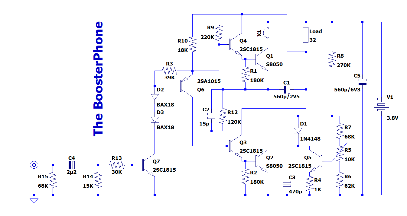
Q7 is the input stage and the VAS. D2 and D3 limit the negative swing, to avoid saturating Q6 and the latching-up of the OP stage. Ordinary 1N4148's also work there, but their forward drop is collectively a few hundreds of mV higher than strictly required, leading to an output swing curtailed by 300mV. Not a lot, but with a 3~4V supply, every mV counts. BAX18 have a higher conductance and optimum drop.
Many other types would be suitable. If Vf is too low, the latchup will manifest itself.
Q6 is the phase-splitter, steering the drive current to the suitable output transistor.
With this topology, the current derived by Q6 would normally be ~half the drive current provided by R18, and most of it would be dumped into a B-E resistor; the same would happen with the upper transistor.
Here, this textbook approach would be wasteful and difficult to compensate against temperature and supply voltage variations, which is why I used an alternative method: there are no B-E resistors, and Q5 shunts the quasi-totality of the current sent by Q6, and Q6 itself takes almost the totality of the current provided by R18.
The tiny remainder serves to bias the OP's under quiescent conditions. The symmetry is respected, since both B-E impedances are now ~infinity, and the quiescent behaviour can be controlled by R4 and the adjustable base divider. Many combinations result in the same CCS current, but the voltage and temperature behaviour can be very different. With a suitable selection, it is possible to compensate almost perfectly the temperature or voltage variation, but not at the same time: some tradeoffs are required
A problem remains: for the negative swing, Q6 needs to send more current into the lower half of the PP, but it already sends all the current it has available, save the quiescent base current of Q4, which is insufficient. The bootstrap arrangement is not a perfect CCS, and leaks some additional current too, but it remains marginal.
R9 is added to provide the 10µA or so required to properly drive the lower half.
The VAS loading resistor is returned to the boostrapped voltage to maximise the output swing.
The OP stage uses darlingtons, because the drive current required to reach the peak output current would be incompatible with the low quiescent power requirement.
Unfortunately, darlingtons suffer from a Vcesat>Vbe, which is unacceptable for a low-voltage amplifier. The workaround is to also tie the collectors of the drivers to the boostrapped voltage.
Lots of components return to the bootstrapped voltage, but the total current doesn't exceed a few tens of µA which has no effect on the heaadphones
The compensating CCS works well under static conditions, but when the upper half is active, its voltage collapses completely, leading to artefacts, especially when it needs to wake up again.
To avoid or reduce these Xover artefacts, an antisaturation diode D1 is included. C3 adds a final touch to smooth out the result, which is relatively convincing when you look at the triangle wave I posted earlier.
The quiescent output voltage is determined by the Vbe of Q7 and the resistors R12 to 14, forming a Vbe multiplier. It is not optimal, as it doesn't track the supply voltage, but improving on that would add complications.
The jumper can be used to adjust the quiescent current. I have used 80µA, but any other value could be chosen: the higher the current, the better the linearity, but the downside is a reduced autonomy.
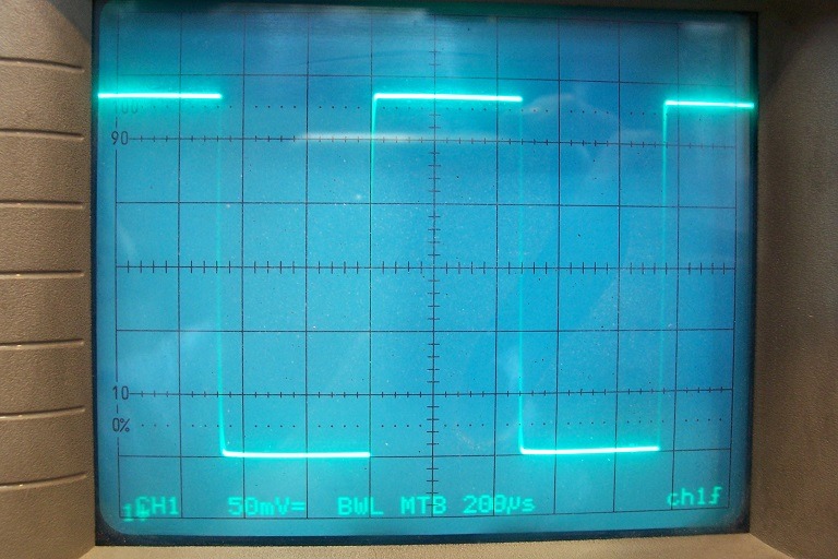
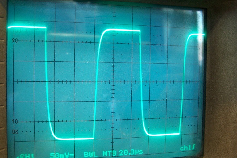
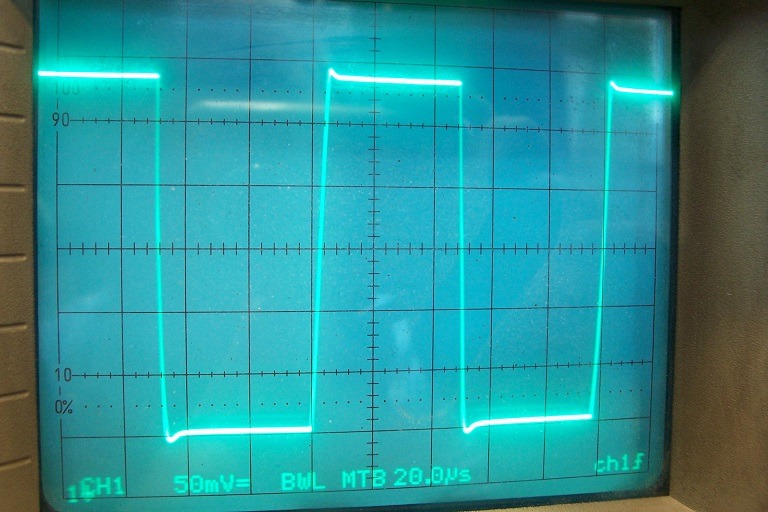
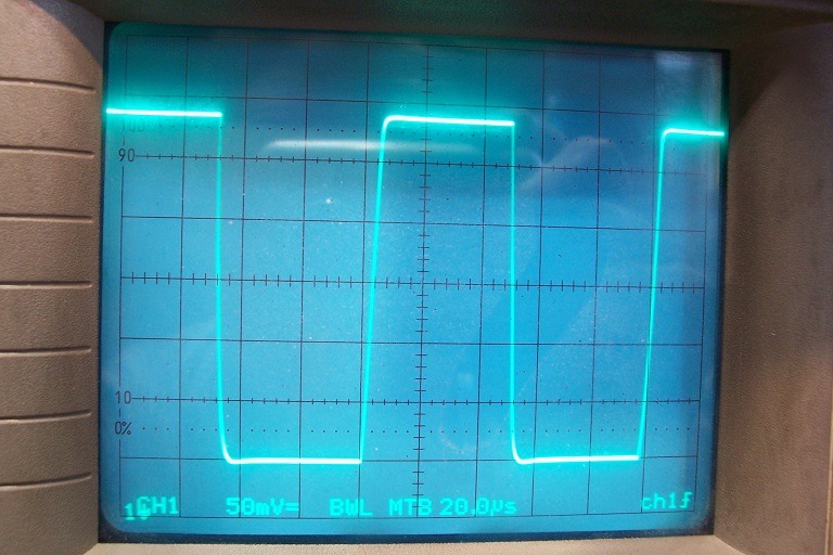
Here are some more oscillograms.
The first is a 1kHz squarewave:
This one is a 10kHz squarewave:
Now, 10kHz without the feedback capacitor:
10kHz with a 2.7pF feedback capacitor:
Q7 is the input stage and the VAS. D2 and D3 limit the negative swing, to avoid saturating Q6 and the latching-up of the OP stage. Ordinary 1N4148's also work there, but their forward drop is collectively a few hundreds of mV higher than strictly required, leading to an output swing curtailed by 300mV. Not a lot, but with a 3~4V supply, every mV counts. BAX18 have a higher conductance and optimum drop.
Many other types would be suitable. If Vf is too low, the latchup will manifest itself.
Q6 is the phase-splitter, steering the drive current to the suitable output transistor.
With this topology, the current derived by Q6 would normally be ~half the drive current provided by R18, and most of it would be dumped into a B-E resistor; the same would happen with the upper transistor.
Here, this textbook approach would be wasteful and difficult to compensate against temperature and supply voltage variations, which is why I used an alternative method: there are no B-E resistors, and Q5 shunts the quasi-totality of the current sent by Q6, and Q6 itself takes almost the totality of the current provided by R18.
The tiny remainder serves to bias the OP's under quiescent conditions. The symmetry is respected, since both B-E impedances are now ~infinity, and the quiescent behaviour can be controlled by R4 and the adjustable base divider. Many combinations result in the same CCS current, but the voltage and temperature behaviour can be very different. With a suitable selection, it is possible to compensate almost perfectly the temperature or voltage variation, but not at the same time: some tradeoffs are required
A problem remains: for the negative swing, Q6 needs to send more current into the lower half of the PP, but it already sends all the current it has available, save the quiescent base current of Q4, which is insufficient. The bootstrap arrangement is not a perfect CCS, and leaks some additional current too, but it remains marginal.
R9 is added to provide the 10µA or so required to properly drive the lower half.
The VAS loading resistor is returned to the boostrapped voltage to maximise the output swing.
The OP stage uses darlingtons, because the drive current required to reach the peak output current would be incompatible with the low quiescent power requirement.
Unfortunately, darlingtons suffer from a Vcesat>Vbe, which is unacceptable for a low-voltage amplifier. The workaround is to also tie the collectors of the drivers to the boostrapped voltage.
Lots of components return to the bootstrapped voltage, but the total current doesn't exceed a few tens of µA which has no effect on the heaadphones
The compensating CCS works well under static conditions, but when the upper half is active, its voltage collapses completely, leading to artefacts, especially when it needs to wake up again.
To avoid or reduce these Xover artefacts, an antisaturation diode D1 is included. C3 adds a final touch to smooth out the result, which is relatively convincing when you look at the triangle wave I posted earlier.
The quiescent output voltage is determined by the Vbe of Q7 and the resistors R12 to 14, forming a Vbe multiplier. It is not optimal, as it doesn't track the supply voltage, but improving on that would add complications.
The jumper can be used to adjust the quiescent current. I have used 80µA, but any other value could be chosen: the higher the current, the better the linearity, but the downside is a reduced autonomy.
Here are some more oscillograms.
The first is a 1kHz squarewave:
This one is a 10kHz squarewave:
Now, 10kHz without the feedback capacitor:
10kHz with a 2.7pF feedback capacitor:
~half the drive current provided by R18
do you refer to R10 (18k)?and Q6 itself takes almost the totality of the current provided by R18
thanks!
Oops! Yes, you are right of course. I need some time offdo you refer to R10 (18k)?
Here is a short description of the BMS section.
The charging part is just a conventional constant I/V supply based on a TL431. The voltage accuracy needs to be good, to avoid any risk with the lithium cell. The one I used has a maximum voltage of 4.2V, but I adjusted the charger at 4.1V, to be on the safe side and minimize the stress. Other types/chemistries may need slightly different voltages, and the adjustment range should cover them.
The constant-current part is defined by R14 at 100mA. The cell tolerates a much higher current, but I do not need a fast charging, and I wanted to avoid a big supply and heat dissipation with this linear charger.
Each mode is indicated by a dedicated LED.
To prevent the cell from discharging into the charger, D5 and Q3 block any possible reverse flow. Q3 disconnects the measuring resistive divider when the charger is disconnected, as it would consume a non-negligible current compared to the amplifiers.
The low-voltage detection is based on a relaxation oscillator built around Q2 and Q4. On its own, the oscillator can oscillate freely for a wide range of supply voltages, but the blue LED D2 limits the charging voltage of the timing capacitor C1, and if the supply is high enough, it blocks the oscillations.
The discharge pulse is amplified by Q1 which drives the indication LED. The Hfe of the transistor limits the current, the LED has no limiting resistor.
The result is a very visible, short (~1ms) and powerful flash at 1.5Hz, but the average consumption remains very low.
When the circuit is inactive, the consumption is governed by the 3.3 meg resistor, and is also very low.
D3 and D4 compensate the numerous junctions of the circuit and the temperature behaviour of the lithium cell.
I have adjusted the indication at 3.5V, but the cell can tolerate 3.2V without damage
Final recommendations and health warnings:
It was mentioned at the beginning of the topic, but a reminder is probably useful: this booster is not aimed at super-quality, exceptional sound; it is just decent and acceptable at a 80µA bias current (for me anyway).
Its purpose is essentially utilitarian: it is a practical and hassle-free solution when you need to boost a weak source (typically a wimpy digital player) used in combination with low-grade, low-efficiency earbuds or headphones, a situation very common nowadays.
Its advantage is simplicity and freedom of maintenance.
If you have a good earphone output and efficient headphones, you certainly don't need it: in fact, you risk shattering your eardrums (litterally!). The voltage gain is 4, meaning a 16x increase in power.
You only have one pair of ears (hopefully), so don't be silly and risk ruining them.
You can improve the sound quality by increasing the quiescent current: with 1mA, the more than tenfold increase will translate into a ~3x better linearity (and a much reduced autonomy, obviously), but it will never be able to compete with the fine class A designs presented in this section.
You can use it as a line-level booster too: that was the main goal of Danny, at the origin of this project.
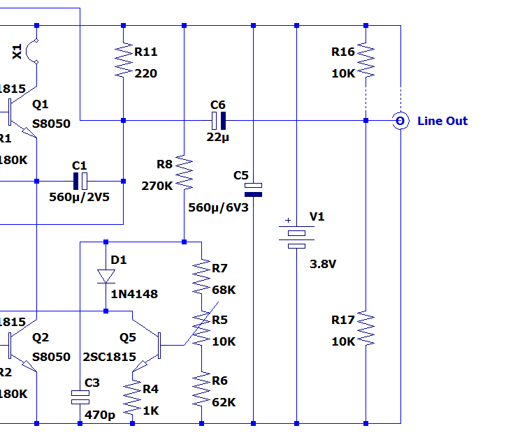
You need a dummy load to simulate the headphones: something between 100ohm and 1K is OK and will greatly improve the linearity. Ideally, you would need to connect the output ground to the + side because the load is referenced there, but if it is not possible (multiple ground interconnections) and if the supply is clean and stiff (like a good rechargeable battery), you can use the - rail too.
This schematic of the output outlines both options. C6 needs to be reversed if you use the +GND option:
Nice to see you back Daniel! I hope everything is alright for you.
You (heavily) inspired this project, and now I find myself using it daily: you are a genius. I felt that I was amiss of something, but I thought that it was just a quirk of mine, not worth materializing.
Now that it is built and working, I enjoy it everyday.
You (heavily) inspired this project, and now I find myself using it daily: you are a genius. I felt that I was amiss of something, but I thought that it was just a quirk of mine, not worth materializing.
Now that it is built and working, I enjoy it everyday.
Thank you for the kindly compliment!
I'm probably not a genius? It took ages for it to dawn on me that my audio troubles were because the source devices just weren't pampered enough to have them in good condition. . . before amplifying that. It was good that you made it an inverting amplifier. I'm curious: Is the input singleton or ntp?
I'm probably not a genius? It took ages for it to dawn on me that my audio troubles were because the source devices just weren't pampered enough to have them in good condition. . . before amplifying that. It was good that you made it an inverting amplifier. I'm curious: Is the input singleton or ntp?
good morning @Elvee ,
I consider implementing your BMS system using a Li-Ion cell but only 5 V (USB) charging voltage. thus I try to avoid any possible voltage drops.
I consider implementing your BMS system using a Li-Ion cell but only 5 V (USB) charging voltage. thus I try to avoid any possible voltage drops.
When simulating the BMS circuit i could not see any significant difference when substituting the reverse flow protection diode D5 with a simple wire. Is there anything I may not be aware of or is the simulator not accurate enough? Thanks in advance!To prevent the cell from discharging into the charger, D5 and Q3 block any possible reverse flow.
indeed... thank you very much, Elvee!1.5 year has passed already
- Home
- Amplifiers
- Headphone Systems
- The BoosterPhone is a convenient and innovative in-line amplifier