Hi !
I've been working on a bluetooth DAC project that I've been thinking about for some time.
After several days of investigation I selected a "simple" architecture based on the PCM5102A chip and a Tinysine TSA5001 bluetooth module.
I chose this chip because it seems to me to be one of the easiest to implement thanks to its integrated clock and pre-amp. Furthermore, I know it because my current DAC is based on it and I like the sound reproduction, although it is a fairly inexpensive DAC.
As for the Bluetooth module, I selected it because it supports aptX-HD and the I2S bus in slave mode, which should allow it to synchronize its clock with that of the DAC, if I understood correctly.
My skills being limited I decided on a simple design but with quality components.
For my design, I tried to respect the reference diagrams as much as possible.
FYI the DAC will be powered by the 12v auxiliary output of my Tripath amp's power supply. I am therefore limited to 2200uF of total capacitance for my DAC, in order to respect the limits of the power supply.
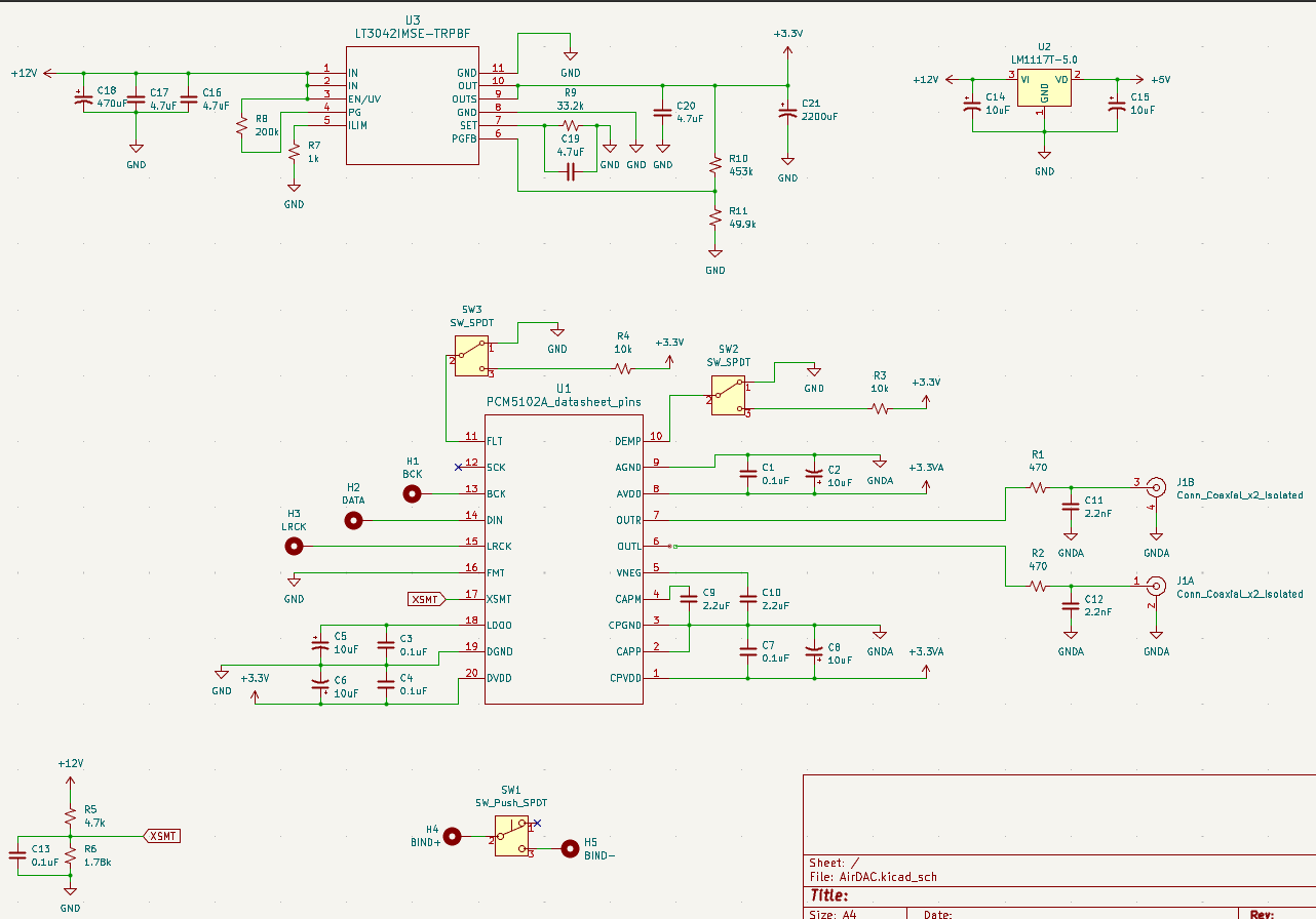
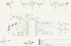
I have just finished the diagram, I would like to have the experts' opinion on its viability and be able to correct any errors that I may have made.
Here is the diagram made with Kicad:
Edit : C21 has wrong value, changed it for 1200uF.
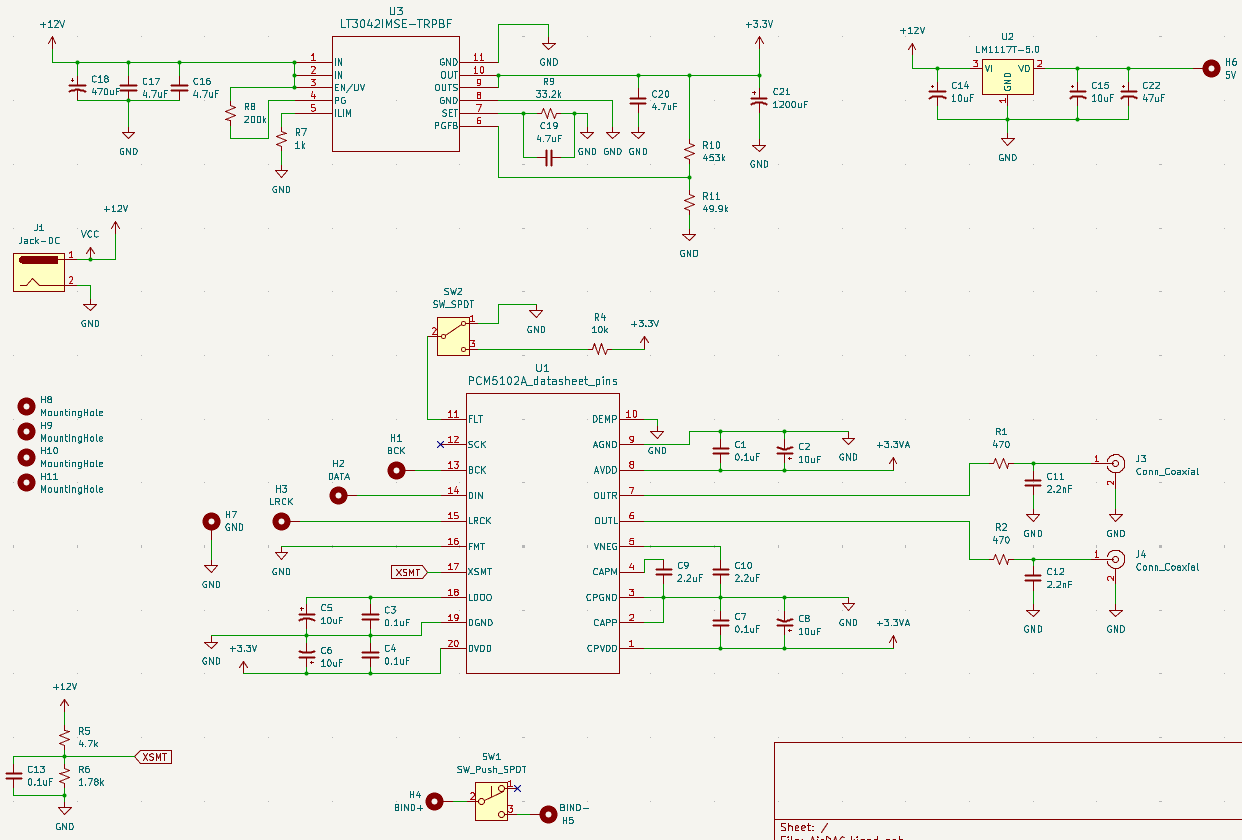
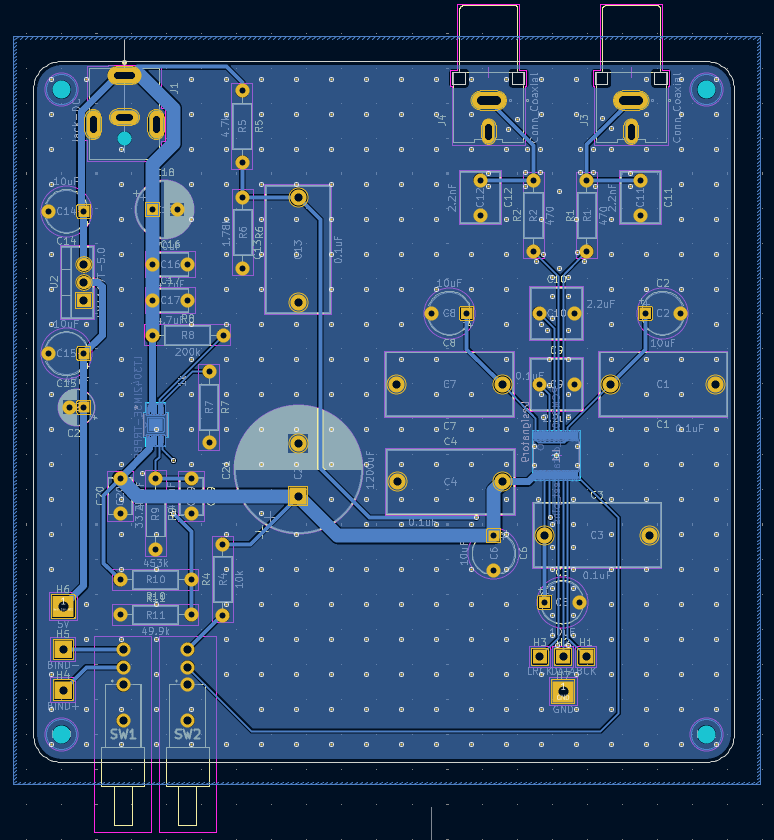
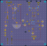
I know the double post is not something very popular but I made good progress on my design, I made corrections to the diagram and I finished the pcb.
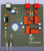
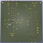
The board measures 100x100mm and the routing and smd components are on the underside.
Kicad reports errors to me but I think they are false positives, telling me that certain circuits are not powered or open.
I'm just wondering if the two right angles on the 3.3v rail might be a problem.
I won't be able to hold off on ordering the pcb and components for long, so if anyone sees any errors and objects to this order, say so now or forever keep quiet
1. "The system clock PLL mode allows designers to use a simple 3-wire I 2S audio source when driving the DAC. The 3-wire source reduces the need for a high frequency SCK, making PCB layout easier, and reduces high frequency electromagnetic interference. The device starts up expecting an external SCK input, but if BCK and LRCK start correctly while SCK remains at ground level for 16 successive LRCK periods, then the internal PLL starts, automatically generating an internal SCK from the BCK reference"
Do not leave sck floating, ground it.
2. Consider adding thermal barriers to the GND plane, otherwise it will be a nightmare to solder the board.
Do not leave sck floating, ground it.
2. Consider adding thermal barriers to the GND plane, otherwise it will be a nightmare to solder the board.
Thank you for your answer !
Since my previous post, I realized that I made a lot of mistakes. Poor understanding of the reference diagram, poor placement of components and poorly optimized routing. Everything had to be redone.
So I corrected the diagram, replaced the 3.3v voltage regulator with a model that was easier to integrate. This having an integrated current limiter, I was able to increase the total capacitance of the DAC without fear for my external 12v power supply.
I also realized that if I used a bluetooth module in I2S slave mode, the PLL of the PCM5102A would not work without an external clock, so I added a TCXO oscillator on the SCK pin.
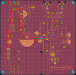
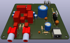
In order to simplify the routing I chose a 4-layer PCB which is barely more expensive than the 2-layer one. The power circuits are on the upper side while the signals and the SMD components are on the lower side.
The mega ground plane is now composed of one plane per copper layer, connected by nearly 400 vias. It's probably overkill, but it doesn't cost more.
I added the thermal brakes as you advised me.
I'm going to wait a few more days before ordering because every time I think everything is ok, I end up discovering an error


I also realized that if I used a bluetooth module in I2S slave mode, the PLL of the PCM5102A would not work without an external clock, so I added a TCXO oscillator on the SCK pin.
That's a bit confusing. I2S slave usually means that the device expects BCK and WCK and PCM5102 could not provide it. I also suggest you to add 22-47 Ohm resistors in series in all I2S and SCLK signals. That actually helps with signal integrity but in your case the most important benefit is during debug.
I guess the layout is okay. However, I have doubts regarding power supply scheme: you have 2 LDOs that convert 12 to 3.3 and 5v. That's means quite a lot of power dissipation on them, even at 10mA it is ~90mW. A little one may not survive. A better solution will be to drop 12V to ~6V on an buck converter and the have two LDO's. Or, if you want to avoid buck, at least put one LDO with a heatsink to drop voltage to 6V and then put another two LDOs to get 5 and 3.3V.
The definition of I2S master is that it generates the clocks. The PCM5102 goes into master mode only if SCLK is present without BCLK at startup I think, from what I read from the datasheet. It also mentions that the device needs to be in "Software Mode" for this, without anywhere explaining this term!
Or it could be that the PLL only allows flexibility in the SCLK frequency in "Software mode"....
Or it could be that the PLL only allows flexibility in the SCLK frequency in "Software mode"....
Mark,
I still think that there is a confusion because usually bt modules are configured to be i2s masters.
Yes, exactly. And from 5102 datasheet I do not see that it can act as a master: bck, lrck pins are inputs only.The definition of I2S master is that it generates the clocks.
I still think that there is a confusion because usually bt modules are configured to be i2s masters.
You are right the 3.3v LDO probably won't survive.That's a bit confusing. I2S slave usually means that the device expects BCK and WCK and PCM5102 could not provide it. I also suggest you to add 22-47 Ohm resistors in series in all I2S and SCLK signals. That actually helps with signal integrity but in your case the most important benefit is during debug.
I guess the layout is okay. However, I have doubts regarding power supply scheme: you have 2 LDOs that convert 12 to 3.3 and 5v. That's means quite a lot of power dissipation on them, even at 10mA it is ~90mW. A little one may not survive. A better solution will be to drop 12V to ~6V on an buck converter and the have two LDO's. Or, if you want to avoid buck, at least put one LDO with a heatsink to drop voltage to 6V and then put another two LDOs to get 5 and 3.3V.
I could put a LM340S-5.0/NOPB which will power both the bluetooth module as well as the 3.3v LDO. So I can remove the LM1117 which would become useless.
I will also add SMD resistors on the I2S wires. More like 22 or 47ohms? And another one between the oscillator and SCK pin ?
I usually put 47 Ohm. Yes, between OSC and SCK pin.More like 22 or 47ohms? And another one between the oscillator and SCK pin ?
Placing via right in the pad is not a good practice: the solder paste would go there and surface tension/solder amount would not be equal on different pads. I know, for hand soldering that does not matter but still
Please also double check oscillator connections. Pin 1 is usually OE, check the datasheet.
Thanks for these tips!
Someone on the Kicad subreddit finds my design 'exotic' and thinks that there are too many large capacitors, especially the WIMA 0.1uF, that it's overkill for a bluetooth DAC, and I think he's right.
I'm going to redo a more reasonable design and take the opportunity to review my power supply circuit and other adjustments that you advised me.
- Home
- Design & Build
- Electronic Design
- Bluetooth DAC project